Notifications
Mark all as read

Zeeko has joined our supplier lineup. Check out their catalog products.

Introducing high-E Photonics! Explore their products on our website.
%20rotate(45)'/%3e%3crect%20class='cls-4'%20x='9.85'%20y='26.36'%20width='38.34'%20height='5.31'%20transform='translate(58.03%2058.03)%20rotate(-180)'/%3e%3cpolygon%20class='cls-4'%20points='17.64%2022.13%2017.64%2016.8%2026.34%2016.8%2026.34%208.1%2031.66%208.1%2031.66%2016.8%2040.37%2016.8%2040.37%2022.13%2017.64%2022.13'/%3e%3cpolygon%20class='cls-4'%20points='17.64%2041.2%2017.64%2035.88%2040.37%2035.88%2040.37%2041.2%2031.67%2041.2%2031.67%2049.9%2026.34%2049.9%2026.34%2041.2%2017.64%2041.2'/%3e%3c/g%3e%3c/g%3e%3c/svg%3e)
Welcome aboard Piezolution! Find their catalog products now featured on MEETOPTICS.

New manufacturer announcement: Get to know SMART Photonics and their latest product offerings.
%20--%3e%3csvg%20version=%271.1%27%20id=%27layer%27%20x=%270px%27%20y=%270px%27%20viewBox=%270%200%20512%2072%27%20xml:space=%27preserve%27%20width=%27512%27%20height=%2772%27%20xmlns=%27http://www.w3.org/2000/svg%27%20xmlns:svg=%27http://www.w3.org/2000/svg%27%3e%3cdefs%20id=%27defs9%27%20/%3e%3cg%20id=%27g10%27%20transform=%27matrix(0.83352366,0,0,0.83352366,-11.170586,-232.01953)%27%3e%3cg%20id=%27g6%27%3e%3cpath%20d=%27m%20130.2,295.4%20h%201.5%20c%201.2,0%202.2,1%202.2,2.2%20V%20340%20c%200,1.2%201,2.2%202.2,2.2%20h%2025%20c%201.2,0%202.2,1%202.2,2.2%20v%201%20c%200,1.2%20-1,2.2%20-2.2,2.2%20h%20-30.9%20c%20-1.2,0%20-2.2,-1%20-2.2,-2.2%20v%20-47.8%20c%20-0.1,-1.2%200.9,-2.2%202.2,-2.2%27%20id=%27path1%27%20/%3e%3cpath%20d=%27m%20193.3,295.4%20h%201.5%20c%201.2,0%202.2,1%202.2,2.2%20v%2047.8%20c%200,1.2%20-1,2.2%20-2.2,2.2%20h%20-1.5%20c%20-1.2,0%20-2.2,-1%20-2.2,-2.2%20v%20-47.8%20c%200,-1.2%201,-2.2%202.2,-2.2%27%20id=%27path2%27%20/%3e%3cpath%20d=%27m%20226.4,321.7%20v%20-0.2%20c%200,-14.3%2010.5,-27%2026.2,-27%207.1,0%2012,1.6%2016.3,4.6%201.8,1.2%202.2,3.6%200.7,5.2%20-0.7,0.9%20-2.1,1%20-3,0.3%20-3.6,-2.8%20-7.9,-4.6%20-14.3,-4.6%20-11.6,0%20-19.9,9.8%20-19.9,21.4%20v%200.1%20c%200,12.5%208,21.7%2020.7,21.7%205.5,0%2010.6,-2%2014.2,-4.6%200.6,-0.4%200.9,-1.1%200.9,-1.8%20v%20-9.7%20c%200,-1.2%20-1,-2.2%20-2.2,-2.2%20h%20-11.5%20c%20-1.2,0%20-2.2,-1%20-2.2,-2.2%20V%20322%20c%200,-1.2%201,-2.2%202.2,-2.2%20h%2017.2%20c%201.2,0%202.2,1%202.2,2.2%20v%2017.6%20c%200,0.6%20-0.3,1.3%20-0.8,1.7%20-4.8,4%20-11.8,7.3%20-20.2,7.3%20-16.3,0%20-26.5,-12%20-26.5,-26.9%27%20id=%27path3%27%20/%3e%3cpath%20d=%27m%20305.9,295.4%20h%2033.4%20c%201.2,0%202.2,1%202.2,2.2%20v%201%20c%200,1.2%20-1,2.2%20-2.2,2.2%20h%20-27.5%20c%20-1.2,0%20-2.2,1%20-2.2,2.2%20v%2013.4%20c%200,1.2%201,2.2%202.2,2.2%20h%2024.1%20c%201.2,0%202.2,1%202.2,2.2%20v%201%20c%200,1.2%20-1,2.2%20-2.2,2.2%20h%20-24.1%20c%20-1.2,0%20-2.2,1%20-2.2,2.2%20v%2013.9%20c%200,1.2%201,2.2%202.2,2.2%20h%2027.8%20c%201.2,0%202.2,1%202.2,2.2%20v%201%20c%200,1.2%20-1,2.2%20-2.2,2.2%20h%20-33.7%20c%20-1.2,0%20-2.2,-1%20-2.2,-2.2%20v%20-47.8%20c%200,-1.3%201,-2.3%202.2,-2.3%27%20id=%27path4%27%20/%3e%3cpath%20d=%27m%20372.3,295.4%20h%202.2%20c%200.7,0%201.3,0.3%201.7,0.8%20l%2028.3,36%20c%201.3,1.6%203.9,0.7%203.9,-1.4%20v%20-33.3%20c%200,-1.2%201,-2.2%202.2,-2.2%20h%201.3%20c%201.2,0%202.2,1%202.2,2.2%20v%2047.8%20c%200,1.2%20-1,2.2%20-2.2,2.2%20h%20-1.4%20c%20-0.7,0%20-1.3,-0.3%20-1.7,-0.8%20l%20-29.1,-37%20c%20-1.3,-1.6%20-3.9,-0.7%20-3.9,1.4%20v%2034.3%20c%200,1.2%20-1,2.2%20-2.2,2.2%20h%20-1.3%20c%20-1.2,0%20-2.2,-1%20-2.2,-2.2%20v%20-47.8%20c%200,-1.2%201,-2.2%202.2,-2.2%27%20id=%27path5%27%20/%3e%3cpath%20d=%27M%20457.1,300.9%20H%20444%20c%20-1.2,0%20-2.2,-1%20-2.2,-2.2%20v%20-1%20c%200,-1.2%201,-2.2%202.2,-2.2%20h%2036.6%20c%201.2,0%202.2,1%202.2,2.2%20v%201%20c%200,1.2%20-1,2.2%20-2.2,2.2%20h%20-13.1%20c%20-1.2,0%20-2.2,1%20-2.2,2.2%20v%2042.4%20c%200,1.2%20-1,2.2%20-2.2,2.2%20h%20-1.6%20c%20-1.2,0%20-2.2,-1%20-2.2,-2.2%20v%20-42.4%20c%200,-1.2%20-1,-2.2%20-2.2,-2.2%27%20id=%27path6%27%20/%3e%3c/g%3e%3cg%20id=%27g8%27%3e%3cpath%20d=%27m%20512.5,295.4%20h%2033.4%20c%201.2,0%202.2,1%202.2,2.2%20v%201%20c%200,1.2%20-1,2.2%20-2.2,2.2%20h%20-27.5%20c%20-1.2,0%20-2.2,1%20-2.2,2.2%20v%2013.4%20c%200,1.2%201,2.2%202.2,2.2%20h%2024.1%20c%201.2,0%202.2,1%202.2,2.2%20v%201%20c%200,1.2%20-1,2.2%20-2.2,2.2%20h%20-24.1%20c%20-1.2,0%20-2.2,1%20-2.2,2.2%20v%2013.9%20c%200,1.2%201,2.2%202.2,2.2%20h%2027.8%20c%201.2,0%202.2,1%202.2,2.2%20v%201%20c%200,1.2%20-1,2.2%20-2.2,2.2%20h%20-33.7%20c%20-1.2,0%20-2.2,-1%20-2.2,-2.2%20v%20-47.8%20c%200,-1.3%201,-2.3%202.2,-2.3%27%20id=%27path7%27%20/%3e%3cpath%20d=%27m%20574.4,321.7%20v%20-0.2%20c%200,-14.8%2011,-27%2026.4,-27%208.4,0%2013.9,2.7%2018.6,6.7%201,0.8%201.1,2.3%200.2,3.2%20l%20-1,1.1%20c%20-0.8,0.9%20-2.1,1%20-3,0.2%20-4,-3.4%20-8.6,-5.8%20-14.9,-5.8%20-11.6,0%20-20.2,9.4%20-20.2,21.4%20v%200.1%20c%200,12.1%208.7,21.6%2020.2,21.6%206.5,0%2010.9,-2.2%2015.4,-6.2%200.9,-0.8%202.2,-0.7%203,0.1%20l%200.7,0.7%20c%200.9,0.9%200.9,2.4%20-0.1,3.2%20-5,4.6%20-10.7,7.5%20-19.2,7.5%20-14.9,0.3%20-26.1,-11.6%20-26.1,-26.6%27%20id=%27path8%27%20/%3e%3c/g%3e%3cg%20id=%27g9%27%3e%3crect%20x=%2753.299999%27%20y=%27284.29999%27%20width=%2741.799999%27%20height=%2741.799999%27%20id=%27rect8%27%20/%3e%3cpolygon%20points=%2720.6,284.3%2020.6,358.8%2077.6,358.8%2077.6,342.2%2037.2,342.2%2037.2,284.3%20%27%20id=%27polygon8%27%20/%3e%3c/g%3e%3c/g%3e%3c/svg%3e)
Introducing LIGENTEC! Explore their photonic foundry service on our website.

LioniX International has joined our supplier lineup. Check out their customized microsystem solutions.

New manufacturer announcement: Get to know Polariton Technologies and their latest custom PIC offerings.

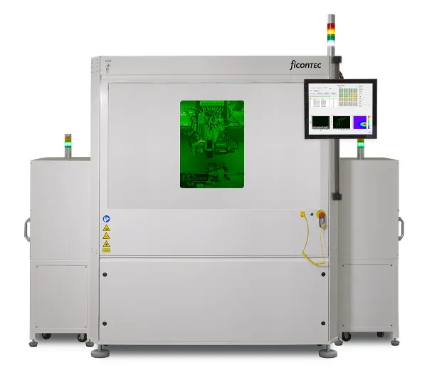
Welcome aboard ficonTEC! Find their catalog products and solutions now featured on MEETOPTICS.
We have a new categorization for Photonic Integrated Circuits. Find all the products from trusted suppliers.

Introducing Yalosys Ltd! Explore their laser microprocessing solutions on our website.

Epiphany has joined our supplier lineup. Check out their photonic design solutions.

New manufacturer announcement: Get to know Light Trace Photonics and their latest product offerings.
- Your cart is empty. Please add some items.


WAFER TESTLINE - WAFER TESTLINE

WAFER TESTLINE
Product Line
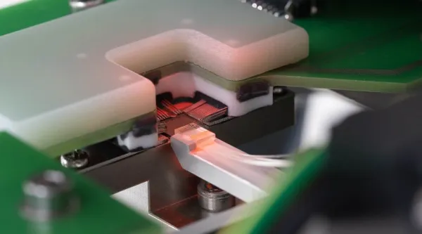
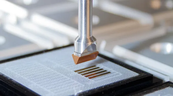
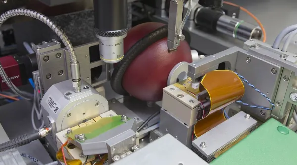
The WAFER TESTLINE product line is a versatile electro-optical test and measurement system platform designed for wafer-level photonic device testing. It features a re-configurable probe-wafer layout that accommodates multiple photonic integrated circuit (PIC) designs on a multi-project wafer (MPW). Ideal for R&D proof-of-concept device testing, WAFER TESTLINE offers state-of-the-art, multi-channel electro-optical testing for on-wafer waveguides and PIC input/output. It includes custom 3D-printed fiber tips that support edge-coupling, enabling low-loss coupling for all optical coupling mechanisms. The system is equally effective for testing multiple singulated devices on suitable carrier formats. In volume manufacturing, WAFER TESTLINE allows for fully automatic testing of all identical devices on a wafer. Its built-in device cataloging and traceability provide comprehensive yield and performance data across entire wafers, offering invaluable feedback for wafer fabrication processes.
Product Specifications
The ficonTEC WAFER TESTLINE is a versatile electro-optical test and measurement system designed for wafer-level photonic device testing. It features a high-precision motion system with 6-axis alignment for optical probing and 3-axis alignment for electrical probing. The system can handle wafers up to 12 inches with various rotation and translation capabilities. Temperature control is maintained with a chuck ranging from +15 to +80 °C. Handling options vary from manual to automated loading, and the system is compliant with ISO 6 cleanroom standards. Available in different configurations, the WAFER TESTLINE is suitable for both R&D and volume manufacturing, offering valuable yield data and device traceability.
- Product Code
- Angular Travel
- ±100°
- Applications
- 3D Scanning
Sensors - Construction
- Rugged steel base production cell
- Housing Dimensions
- 1800 x 1200 x 2000 mm (WT2000)
1200 x 1200 x 2000 mm (WT1200)
1600 x 1200 x 2000 mm (WT1600)
800 x 1200 x 2000 mm (WT800) - Key Features
- Superior Test Data Acquisition Over Manual Approach
Wafer Fabs Receive PIC Yield Data Across Entire Wafer - Machine Vision
- System referencing and observation camera options
Device and I/O port referencing - Maximum Alignment Time
- 4 s (Vertical, Edge)
- Minimum Connections
- 120 VAC (or country specific)
Air/vacuum
100 Mbit/s network - Motion System
- Multiple optical probing with 6-axis high-precision alignment
Electrical probing with 3-axis alignment - Operating Temperature
- 15 - 80 °C
- Software Features
- Flexible and powerful process programming
Extended operator-less control - Supported Wafer Size
- < 304.8 mm (12", WT1600, WT2000, WT1200)
< 101.6 mm (4", WT800) - Temperature Accuracy
- ±0.1 °C
- Type of Movement
- Rotary, XY Translation
- Supplier Location
- Germany
Technical Documents
